
You order a batch of LEDs. The samples look perfect. Three months later, your installation starts flickering like a broken neon sign. The brightness drops. The colors shift. Your client calls, angry. You check everything—power supply, wiring, installation—all fine. The problem? The LEDs themselves are failing. This is not a defect. This is what happens when manufacturing process control fails.
LEDs are not simply "made"—they are precision-engineered through controlled material selection, chip binning, encapsulation chemistry, and thermal pathway design. A single parameter drift during production can cause inconsistent brightness, accelerated light decay, and premature failure across an entire batch.

I have worked with manufacturers for years. I have seen projects collapse because the factory could not maintain consistent binning standards. I have tested batches where half the LEDs aged twice as fast as the other half—same design, same supplier, different production runs. The difference was not in the design. It was in the manufacturing discipline.
What Is the Core Process of LED Manufacturing?
You might think LED production is about assembling chips and wires. That is only half the story. The real challenge is maintaining parameter stability across thousands of units. A small shift in encapsulation temperature, a slight variation in chip bin selection, or inconsistent thermal interface application—any of these can destroy long-term performance.
LED manufacturing involves epitaxial wafer growth, chip dicing and binning, die attachment to substrates, wire bonding, phosphor coating (for white LEDs), encapsulation with silicone or epoxy, and final testing under controlled thermal and electrical stress. Each step must be locked to tight tolerances, or the product will degrade unpredictably in real-world use.

The process starts with semiconductor crystal growth. This is where the LED's fundamental electrical properties are defined. Gallium nitride (GaN) substrates are grown layer by layer using metal-organic chemical vapor deposition (MOCVD). The thickness and doping concentration of each layer determine the wavelength and efficiency of the emitted light. After growth, the wafer is diced into thousands of individual chips. These chips are not identical. They vary in brightness, forward voltage, and color temperature. This is why binning exists.
Binning is the sorting process where chips are grouped by measured performance. A professional manufacturer bins by luminous intensity, forward voltage, and chromaticity coordinates. If a project uses mixed bins, the brightness and color will drift over time. This is not a theory. I have seen entire installations fail because the factory used leftover bins to fill orders. The initial samples were fine. The bulk shipment was inconsistent. The client lost trust. The contract was canceled.
After binning, the chips are mounted onto metal-core PCBs or ceramic substrates using die-attach adhesives. The adhesive must be thermally conductive but electrically insulating. If the adhesive layer is too thick, thermal resistance increases. The chip runs hotter. The light output drops faster. If the adhesive is too thin, mechanical stress during thermal cycling can crack the bond. This is why die-attach process control is critical. Temperature, pressure, and cure time must be monitored on every production line.
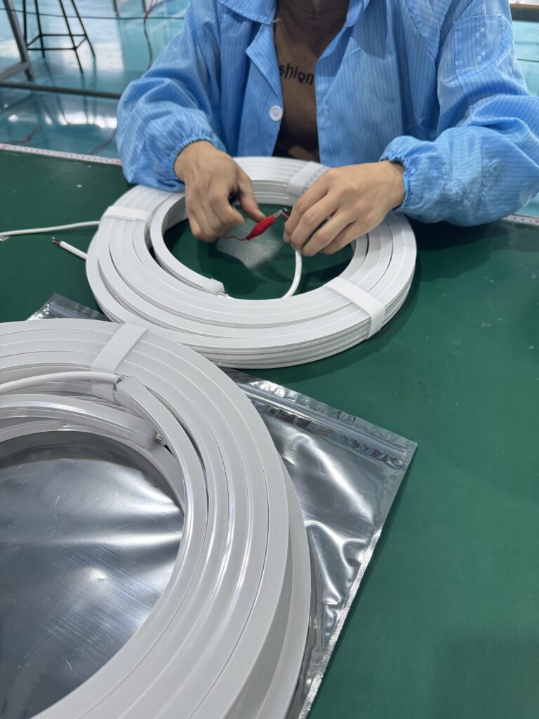
Wire bonding connects the chip to external electrodes. Gold or aluminum wires are ultrasonically welded to the chip surface. The bond must be strong enough to survive thermal expansion cycles but gentle enough to avoid damaging the fragile semiconductor junction. A weak bond will fail under thermal stress. A rough bond will create electrical resistance, generating heat and accelerating degradation.
For white LEDs, a phosphor coating is applied over the blue LED chip. The phosphor converts part of the blue light into yellow, creating white light. The phosphor layer thickness determines the color temperature. A thicker layer produces warmer white. A thinner layer produces cooler white. If the phosphor application is inconsistent, the color temperature will vary across the batch. This is why automated dispensing systems with closed-loop feedback are essential for high-volume production.
Encapsulation is the final sealing step. The LED assembly is covered with a transparent silicone or epoxy resin. This protects the chip from moisture, UV radiation, and mechanical damage. The encapsulant must be thermally stable. Low-quality resins yellow under UV exposure. High-quality silicones remain clear for years. The curing temperature and time must be controlled. Undercured resin will degrade. Overcured resin will crack under thermal cycling. This is not a minor detail. This is the difference between a 5-year lifespan and a 2-year failure.
Why Do Sample LEDs Perform Differently from Mass Production Batches?
You test a sample. It works perfectly. You place a bulk order. The performance drops. The brightness is lower. The color shifts. The light decay accelerates. This is the most common failure pattern in LED procurement. The sample was hand-picked. The bulk production was not.
Sample LEDs are often selected from the tightest bin, assembled with the best materials, and tested under ideal conditions. Mass production batches, however, are subject to material lot variations, equipment drift, and operator inconsistencies. Without strict process control, the production yield will include units that meet specifications on paper but fail prematurely in real-world use.

The root cause is process variation. In a controlled factory, every LED is assembled under the same temperature, humidity, and material conditions. The chip bin is locked. The phosphor thickness is monitored. The encapsulation cure profile is recorded. In an uncontrolled factory, these parameters drift. The chip bin changes because the supplier ran out of the specified grade. The phosphor dispenser clogs, creating uneven coating. The curing oven temperature fluctuates because the heating element is aging.
I have audited factories where the same product line produced LEDs with 30% brightness variation between morning and afternoon shifts. The cause was simple: the air conditioning failed, the workshop temperature rose, and the encapsulant viscosity changed. The dispensing system could not compensate. The phosphor layer became too thick. The color temperature shifted. The factory shipped the batch anyway because the customer did not specify thermal cycling tests.
This is why accelerated aging tests are mandatory. A professional manufacturer runs high-temperature operating life (HTOL) tests at 85°C or higher for at least 1000 hours. This simulates years of real-world use. If the light output drops more than 10% during this test, the production process is out of control. If the color shift exceeds 0.007 in CIE chromaticity coordinates, the phosphor application is inconsistent. These tests are not optional. They are the only way to detect process drift before the product reaches the customer.
Another critical factor is thermal management design. The LED chip generates heat. If the heat cannot escape, the junction temperature rises. High junction temperature accelerates material degradation. The phosphor yellows. The encapsulant cracks. The wire bonds weaken. A well-designed LED has a thermal resistance below 10°C/W from junction to ambient. A poorly designed LED exceeds 20°C/W. The difference is the copper thickness on the PCB, the thermal interface material between the chip and the board, and the heat sink design.
I have tested LED strips where the junction temperature reached 120°C under normal operating conditions. The manufacturer claimed the LEDs were rated for 50,000 hours. In reality, they failed after 10,000 hours. The light output dropped by 50%. The color shifted from neutral white to sickly yellow. The customer blamed the power supply. The real problem was the PCB design. The copper layer was too thin. The thermal vias were missing. The LEDs were cooking themselves.
What Are the Key Parameters That Must Be Controlled During LED Production?
You cannot control what you do not measure. LED manufacturing is not about following a recipe. It is about locking critical parameters and monitoring them continuously. If a factory cannot explain their binning strategy, their encapsulation cure profile, or their thermal resistance targets, they do not have process control. They have guesswork.
The five critical parameters in LED production are chip bin selection, die-attach thermal resistance, phosphor layer uniformity, encapsulation material stability, and junction temperature under rated power. Any deviation in these parameters will cause performance drift, accelerated aging, or premature failure.

| Parameter | Specification | Impact of Drift | Control Method |
|---|---|---|---|
| Chip Bin | Luminous flux ±5%, Vf ±0.1V | Brightness inconsistency, color shift | Automated optical sorting, locked supplier bins |
| Die-Attach Thermal Resistance | <5°C/W | Junction temperature rise, accelerated aging | Controlled adhesive thickness, pressure monitoring |
| Phosphor Layer Thickness | ±10 µm | Color temperature variation, CRI shift | Precision dispensing, real-time thickness measurement |
| Encapsulation Cure Profile | 150°C ±5°C, 2 hours ±10 min | Yellowing, cracking, moisture ingress | Oven temperature logging, time-stamped batch tracking |
| Junction Temperature | <100°C at rated power | Light decay, color shift, bond failure | Thermal simulation, in-situ temperature testing |
Chip binning is the first line of defense. A professional manufacturer sources chips from a single production lot with tight binning tolerances. They do not mix bins. They do not substitute bins when inventory runs low. They halt production and wait for the correct bin to arrive. This is expensive. This is also the only way to guarantee consistent performance.
Die-attach thermal resistance determines how efficiently heat flows from the chip to the substrate. A high-quality die-attach uses silver-filled epoxy or eutectic solder. The bond line thickness is controlled to within 10 µm. The curing temperature is ramped slowly to avoid thermal stress. A low-quality die-attach uses generic epoxy with poor thermal conductivity. The bond line is thick and uneven. The thermal resistance is high. The LED runs hot. The lifespan drops.
Phosphor layer uniformity affects color consistency. A precision dispenser deposits a controlled volume of phosphor slurry onto each chip. The slurry viscosity is temperature-dependent, so the dispenser is climate-controlled. After dispensing, the phosphor is cured under UV light or heat. If the cure is incomplete, the phosphor will degrade under blue light exposure. If the cure is excessive, the phosphor will crack. The cure profile must be validated for every phosphor batch.
Encapsulation material stability is the final barrier against environmental degradation. High-quality silicone resins are formulated to resist UV yellowing, thermal expansion, and moisture absorption. Low-quality epoxy resins yellow within months under outdoor UV exposure. The encapsulant must be cured at the correct temperature for the correct time. Undercured resin is soft and absorbs moisture. Overcured resin is brittle and cracks under thermal cycling. The cure profile must be logged and traceable to each production batch.
Junction temperature is the ultimate performance limiter. Every 10°C increase in junction temperature reduces the LED lifespan by approximately 50%. A well-designed LED operates at 80°C junction temperature under rated power. A poorly designed LED exceeds 110°C. The difference is thermal pathway optimization—copper PCB thickness, thermal vias, heat sink design, and airflow management. A factory that cannot measure junction temperature during production cannot guarantee long-term reliability.
How Can You Verify That an LED Manufacturer Has Real Process Control?
You visit a factory. The production line looks clean. The equipment looks modern. The sales team shows you certifications. You place an order. Six months later, the LEDs fail. What went wrong? You did not verify process control. You verified appearances.
A manufacturer with real process control can show you bin tracking records, thermal resistance test data, accelerated aging reports, and process capability indices (Cpk) for every critical parameter. If they cannot provide this data, they are not controlling the process—they are hoping for the best.

Ask for bin traceability. A professional manufacturer can trace every LED back to its original wafer lot, chip bin, and assembly date. They maintain a database linking serial numbers to process parameters. If a batch fails, they can identify the root cause within hours. If a factory cannot provide this traceability, they are mixing bins, substituting materials, and gambling with your project.
Ask for thermal resistance measurements. A controlled manufacturer tests thermal resistance on every production batch using JEDEC JESD51 standards. They measure the temperature rise from junction to case under rated power. They calculate the thermal resistance and compare it to the design specification. If the measured value exceeds the target by more than 10%, they investigate the die-attach process. If a factory does not measure thermal resistance, they have no idea how their LEDs will perform under real-world thermal stress.
Ask for accelerated aging data. A serious manufacturer runs HTOL tests at 85°C or higher for at least 1000 hours. They measure light output, color shift, and forward voltage at regular intervals. They calculate the projected L70 lifetime (time to 70% light output). They share this data with customers. If a factory refuses to provide aging data, they have not tested their own products. They are selling based on datasheets, not real performance.
Ask for process capability analysis. A world-class manufacturer tracks Cpk values for every critical parameter. Cpk measures how well a process stays within specification limits. A Cpk of 1.33 or higher means the process is stable and capable. A Cpk below 1.0 means the process is out of control. If a factory does not track Cpk, they are not managing process variation. They are reacting to failures after they happen.
I have worked with factories that could not answer these questions. They had nice showrooms. They had ISO certificates on the wall. They had no idea what was happening on their production lines. I have also worked with factories that could pull up real-time process data on a tablet. They showed me bin distribution charts. They showed me thermal resistance trends. They showed me aging test curves. These factories charged more. They also delivered consistent quality.
The difference is not equipment. The difference is discipline. A controlled factory treats every parameter as a variable that must be locked. An uncontrolled factory treats manufacturing as a black box. You put in materials. You get out LEDs. You hope they work. This is not manufacturing. This is gambling.
Conclusion
LED manufacturing is not about assembling chips—it is about controlling process variables that determine long-term reliability. Without strict binning, thermal management, and material stability, even the best design will fail in production.