
You've probably been burned by LED failures that looked perfect on paper. The chips passed. The encapsulant passed. Even the silicone housing cleared QC. Yet three months into deployment, you're staring at catastrophic light decay, cracked packages, and water ingress. Sound familiar?
LED manufacturing1 relies on four core material systems: semiconductor chips2 (GaN/InGaN), encapsulants (silicone/epoxy), substrates (ceramic/metal-core PCB), and outer housings (extruded silicone3). The real challenge isn't picking "good" materials—it's engineering them to age together without tearing each other apart through thermal mismatch and interface failure4.

Here's what most datasheets won't tell you: LED failure is a team sport. Every material layer is simultaneously expanding, contracting, and degrading at different rates. When those rates don't sync up, physics wins and your product loses. Let me walk you through what actually matters beyond the spec sheets.
What semiconductor materials form the LED chip core?
The chip is where photons are born, but it's also where material science gets brutally unforgiving. You can't fake your way through semiconductor selection.
LED chips use Gallium Nitride5 (GaN) or Indium Gallium Nitride5 (InGaN) epitaxial layers grown on sapphire or silicon carbide substrates. Blue/white LEDs require InGaN quantum wells, while red/amber variants use AlInGaP compounds. Substrate choice directly impacts thermal conductivity6 and long-term reliability.

Why substrate material determines your failure timeline
The substrate isn't just a platform. It's a thermal highway that either saves or kills your LED under sustained operation.
Sapphire substrates dominate consumer-grade LEDs due to low cost, but they conduct heat poorly (thermal conductivity6 ~35 W/m·K). Silicon carbide (SiC) substrates offer 3–4× better thermal performance (~120 W/m·K) but cost significantly more. For high-power applications—like our silicone neon flex7 running 15W/m continuously—SiC-based chips prevent junction temperature runaway that causes rapid phosphor degradation8.
Here's the critical part: substrate thermal expansion coefficient9 (CTE) must closely match the GaN epilayer (~5.6 ppm/°C). Excessive CTE mismatch generates mechanical stress during thermal cycling10, leading to microcrack formation at the chip-substrate interface. These cracks propagate slowly over months, creating current leakage paths and localized hotspots that accelerate phosphor yellowing.
| Substrate Material | Thermal Conductivity (W/m·K) | CTE (ppm/°C) | Best Use Case |
|---|---|---|---|
| Sapphire (Al₂O₃) | 35 | 7.5 | Cost-sensitive indoor lighting |
| Silicon Carbide (SiC) | 120 | 4.2 | High-power outdoor/architectural |
| Silicon (Si) | 150 | 2.6 | Large-area integration (experimental) |
We specify SiC-based chips for clients running 24/7 facade lighting in Dubai's +60°C ambient conditions. The upfront cost premium pays back through extended L70 lifespan (>50,000 hours vs. 30,000 on sapphire).
What encapsulation materials protect the LED chip?
Encapsulants are the invisible bodyguards of your LED. Choose wrong, and they'll be the first to betray you under UV and heat.
Silicone encapsulants (methyl/phenyl silicone resins) dominate high-reliability applications due to superior UV resistance11 and thermal stability (-40°C to +150°C). Epoxy resins offer lower cost but yellow rapidly under blue light exposure, making them unsuitable for outdoor or high-intensity applications.

The hidden interface war: encapsulant-to-silicone bonding
This is where 80% of "mysterious" LED failures originate. The encapsulant and outer silicone housing seem compatible in isolation, but under thermal cycling10, their interface becomes a delamination12 zone.
Silicone encapsulants have CTE around 300 ppm/°C. Our extruded silicone3e neon flex](https://siluxa.com/)%%%FOOTNOTE_REF_7%%% housing has CTE around 250 ppm/°C. That 50 ppm/°C differential doesn't sound dramatic until you run 10,000 thermal cycles (day/night, on/off) over 18 months. Each cycle introduces micro-shear forces at the bond line.
Without proper surface treatment, this interface debonds. Once air gaps form, moisture vapor infiltrates, phosphor conversion efficiency drops, and you get the dreaded "dark spots" in what should be seamless linear lighting.
Our manufacturing process includes:
- Plasma surface activation on the silicone housing before chip mounting to increase surface energy
- Silane coupling agents applied to create chemical bridges13 between encapsulant and housing
- Dual-cure encapsulants (heat + UV) to ensure complete polymerization at the interface
- Accelerated aging validation with 1,000-hour 85°C/85%RH testing to prove bond integrity
We learned this the hard way. Three years ago, a European distributor returned 5,000 meters of our early-generation side-view neon flex with interface delamination12. The encapsulant spec was perfect. The silicone spec was perfect. But we hadn't engineered the system. That failure cost us €40,000 and taught us that materials don't exist in isolation.
What substrate materials support the LED assembly?
The substrate is the structural backbone and thermal manager. Cheap out here, and you're building on a foundation of sand.
Metal-Core Printed Circuit Boards14 (MCPCB) with aluminum or copper bases provide essential heat spreading for high-density LED arrays. Ceramic substrates (alumina/aluminum nitride) offer superior thermal performance and electrical isolation but at premium cost. FR4 PCBs remain viable only for low-power decorative applications.

Why aluminum MCPCB is our default for silicone neon flex7
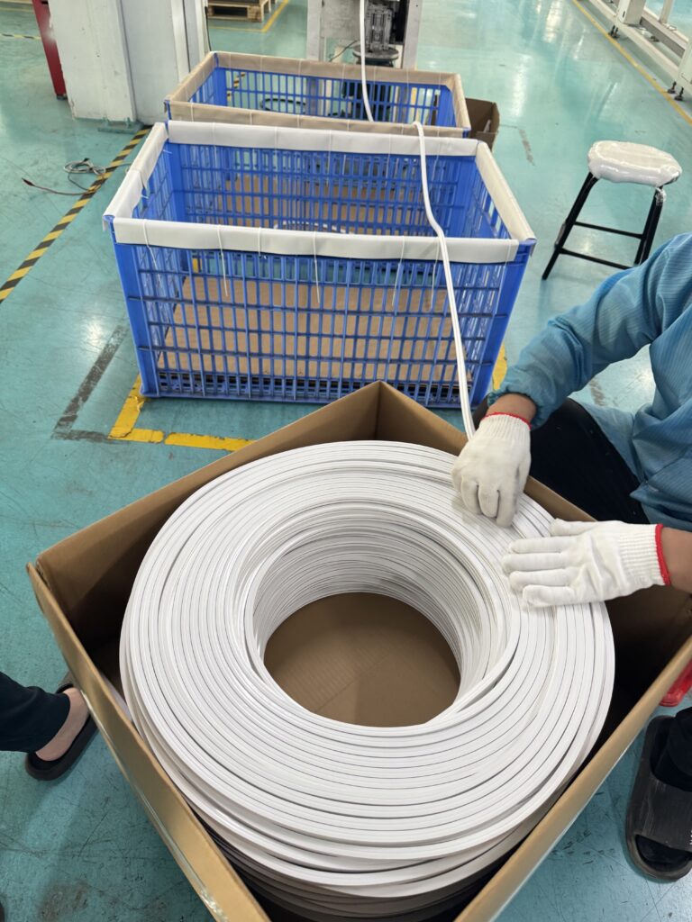
Linear lighting creates unique thermal challenges. Unlike discrete LED modules with localized hotspots, our silicone neon flex7 runs 120 LEDs per meter in continuous extrusion. Heat must spread laterally across the entire length, not just dissipate vertically.
Aluminum MCPCB (1.5mm thickness, 1–2 W/m·K dielectric layer) provides the best cost-performance balance. The aluminum base conducts heat longitudinally along the flex strip, preventing localized junction temperature spikes that would occur with FR4 substrates (thermal conductivity6 ~0.3 W/m·K).
Copper MCPCB offers ~400 W/m·K base conductivity (vs. ~200 W/m·K for aluminum) but adds 40% weight and 60% cost. For architectural installations where weight matters—think suspended ceiling coves or tensioned facade mounting—aluminum wins.
Ceramic substrates (alumina at ~24 W/m·K) would be ideal thermally, but they're rigid and brittle. Our silicone neon flex7 must bend to 50mm radius for intricate signage work. Ceramics crack under repeated flexing. We've tested laser-scored ceramic substrates for flexibility, but yield rates were unacceptable for volume production.
The critical spec: thermal resistance from junction to board must stay below 8°C/W for our 0.5W-per-LED design. This keeps junction temperature under 85°C even at 60°C ambient, preserving phosphor integrity for 50,000+ hour L70 performance.
What outer housing materials ensure long-term durability?
The outer housing is your last line of defense against the environment. This is where material chemistry meets real-world abuse.
Extruded silicone (100% high-molecular-weight PDMS15) provides IP68 waterproofing, UV stability, and flexibility across -40°C to +60°C operating range. PVC and TPU alternatives yellow within 12–18 months under UV exposure and become brittle in freezing conditions, making them unsuitable for architectural-grade installations.

The anti-yellowing challenge: why molecular weight matters
Silicone isn't just "silicone." Low-molecular-weight silicones (used in cheap neon flex knockoffs) have shorter polymer chains that photo-oxidize rapidly under UV-B exposure (280–315 nm wavelength). This oxidation creates carbonyl groups that absorb blue light, causing progressive yellowing.
We specify high-molecular-weight polydimethylsiloxane (PDMS) with average chain lengths exceeding 10,000 units. Longer chains resist UV scission through better energy distribution across the polymer network. Our formulation includes:
- UV-stabilizing additives (hindered amine light stabilizers) at 0.5% concentration
- Cerium oxide nanoparticles (50 nm) that absorb UV-A/B wavelengths before they reach the polymer chains
- Anti-oxidant packages (phenolic compounds) that scavenge free radicals generated during thermal cycling10
Third-party accelerated aging (QUV-A 340 nm, 0.89 W/m², 1,000 hours) shows our silicone maintains >95% light transmittance with zero yellowing. Competing PVC-based products drop to 70% transmittance with visible color shift after just 500 hours.
But here's the system-level insight: silicone housing CTE must be validated with the encapsulant and MCPCB underneath. We've seen cases where premium silicone performed beautifully in standalone testing but cracked after 6 months in production because the underlying MCPCB had mismatched expansion characteristics.
The salt-spray survival test: coastal installation requirements
Coastal projects—marina walkways, beachfront hotels, seaside promenades—expose LEDs to salt fog that accelerates corrosion and material degradation. Standard IP65 ratings don't cut it.
Our silicone formulation passes 1,000-hour salt spray testing16 (ASTM B117, 5% NaCl solution, 35°C) with zero performance degradation. The key is hydrophobic surface chemistry. Silicone's methyl groups create a low-surface-energy barrier (contact angle >110°) that prevents saltwater from wetting the surface and penetrating microscopic imperfections.
We delivered 8,000 meters of top-view silicone neon flex7 to a resort in Phuket, Thailand. After two monsoon seasons and constant salt exposure, the client reported zero failures. The competitive PVC product they'd initially tested failed within 4 months due to plasticizer leaching and subsequent cracking.
How do material interactions cause system-level LED failures?
Individual materials can pass every test and still create catastrophic failures when combined. This is the part that keeps me up at night.
LED system failure originates from CTE mismatch, interface adhesion breakdown, and non-synchronized aging across chip-encapsulant-substrate-housing layers. Thermal cycling induces cumulative mechanical stress that manifests as encapsulant cracking, delamination12, phosphor degradation8, and water ingress after 3–6 months of operation.

The thermal expansion mismatch cascade
Let's walk through a real failure mode we diagnosed last year for a signage manufacturer in Berlin:
Symptoms: After 4 months of 18-hour daily operation, 15% of installed units showed localized dark spots and color temperature shift from 3000K to 4200K.
Root cause analysis:
The client had sourced components separately:
- Chips on sapphire substrates17 (CTE: 7.5 ppm/°C)
- Epoxy encapsulant (CTE: 60 ppm/°C)
- Aluminum MCPCB (CTE: 23 ppm/°C)
- Our silicone housing (CTE: 250 ppm/°C)
During each thermal cycle (ambient 15°C to junction 85°C, ΔT = 70°C), the encapsulant expanded 8× more than the sapphire chip. Over thousands of cycles, this differential expansion created micro-cracks in the encapsulant directly above the chip die.
These cracks allowed moisture ingress to the phosphor layer. Water vapor reacts with YAG:Ce phosphor (the yellow coating that converts blue light to white), causing irreversible degradation and the observed color shift.
Our solution: Switched to silicone encapsulant (CTE: 300 ppm/°C) with added stress-relief additives and implemented a graded-modulus interface layer between chip and bulk encapsulant. This distributed thermal stress over a larger volume, preventing crack initiation. Failures dropped to <0.1%.
Why accelerated aging must test the complete assembly
Standard material testing evaluates components in isolation: chip burn-in, encapsulant UV exposure, silicone salt spray. But these tests miss interaction effects.
Our validation protocol includes:
- Thermal shock cycling (-40°C to +85°C, 1,000 cycles) on complete assembled units
- UV + humidity + heat combined exposure (QUV 340 nm + 85°C/85% RH, 1,000 hours)
- Mechanical flexure testing (50mm bend radius, 10,000 cycles) while electrically powered
- Salt spray with electrical bias (1,000 hours ASTM B117 while operating at rated current)
Only after passing these system-level tests do we release a material combination for production. Single-material certifications mean nothing if the assembly fails.
The supply chain blindness problem
Here's the uncomfortable truth: most LED manufacturers optimize each material independently without system-level ownership. The chip supplier maximizes luminous efficacy. The encapsulant supplier minimizes cost. The PCB fabricator chases yield. Nobody is responsible for how these materials age together over 50,000 hours.
We've vertically integrated critical processes to control this:
- In-house silicone extrusion with real-time viscosity monitoring
- Direct partnerships with chip suppliers for custom CTE-matched encapsulant formulations
- MCPCB fabrication with controlled copper thickness (35 μm ±5%) to manage thermal resistance consistency
When a client asks, "Why does your silicone neon flex7 cost 18% more than the competition?" the answer is this: we're not selling materials. We're selling a validated system where every material is engineered to age gracefully with its neighbors for 5+ years. That engineering costs money upfront but saves fortunes in warranty claims and reputation damage.
Conclusion
LED material selection isn't about picking the "best" chip or encapsulant—it's about engineering a thermal and chemical harmony across four interacting systems. Master the interfaces, validate the complete assembly, and you'll build lighting that survives reality, not just datasheets.
Explore best practices in LED manufacturing to ensure quality and longevity in your products. ↩
Learn about different semiconductor chips used in LEDs to make informed choices for your projects. ↩
Understand the properties of extruded silicone and its role in LED durability. ↩
Explore the causes of interface failure in LED systems to prevent future issues. ↩
Discover the significance of Gallium Nitride in LED technology and its advantages. ↩
Understand the impact of thermal conductivity on LED performance and reliability. ↩
Explore the applications of silicone neon flex in modern lighting solutions. ↩
Understand the factors leading to phosphor degradation in LEDs to enhance product life. ↩
Learn how thermal expansion coefficient affects LED performance and longevity. ↩
Discover the effects of thermal cycling on LED performance and reliability. ↩
Learn about the importance of UV resistance in extending LED lifespan. ↩
Find out how to prevent delamination in LED encapsulation for better performance. ↩
Explore the concept of chemical bridges in LED encapsulation for improved adhesion. ↩
Discover the benefits of Metal-Core Printed Circuit Boards for LED applications. ↩
Learn about high-molecular-weight PDMS and its advantages in LED applications. ↩
Learn about salt spray testing and its importance for LEDs in coastal environments. ↩
Discover the role of sapphire substrates in LED technology and their limitations. ↩