
You probably think LED manufacturing is all about cutting-edge automation and chip precision. But after dealing with a $2.3M architectural lighting failure, I learned the hard truth: the real question isn't how LEDs are made—it's what invisible defects get locked into the product during manufacturing that won't surface until year three of your project.
LED lights are manufactured through a multi-stage process: chip fabrication → die bonding → wire bonding → phosphor coating → encapsulation → SMT assembly → final product integration. However, what most specification sheets won't tell you is that each manufacturing step introduces material stresses, contamination risks, and interface defects that determine whether your system lasts 5 years or fails at 18 months.

I'm writing this because I've seen too many engineers select LED products based on brand names and LM-80 reports, only to face catastrophic field failures that stem directly from manufacturing decisions made months earlier. Let me show you what really happens inside a professional LED production facility—and what you should be asking your supplier.
What Actually Happens During LED Chip Fabrication?
Most people assume LED manufacturing starts when the chip arrives at the packaging factory. Wrong. The foundation of LED reliability is established during the wafer-level fabrication process, where microscopic decisions create invisible time bombs.
LED chip fabrication begins with epitaxial growth on sapphire substrates, followed by mesa etching, electrode deposition, and singulation. The critical failure point isn't the visible chip itself—it's the buried interface between the semiconductor layers and the metal contacts, where thermal expansion mismatch creates cumulative stress with every power cycle.

Here's what happens in a typical Tier-1 LED chip factory:
Stage 1: Epitaxial Layer Growth (MOCVD Process)
The LED wafer starts as a 2-inch or 4-inch sapphire substrate. Inside a Metal-Organic Chemical Vapor Deposition (MOCVD) reactor, multiple quantum well layers are deposited at 1000°C+. The thickness tolerance must stay within ±2nm—any deviation creates wavelength variation.
But here's the hidden issue: thermal stress accumulation. Sapphire has a CTE (Coefficient of Thermal Expansion) of ~7.5 ppm/°C. Gallium Nitride (GaN) is ~5.6 ppm/°C. Every heating and cooling cycle during growth embeds residual stress into the crystalline structure. This stress doesn't break the chip immediately—it creates lattice dislocations that accelerate degradation over thousands of operational hours.
Stage 2: Electrode Formation and Contact Integrity
After mesa etching defines the chip geometry, metal electrodes (typically Ti/Al/Ti/Au multilayers) are deposited via sputtering. The industry standard contact resistance target is <10⁻⁴ Ω·cm². Sounds excellent, right?
The problem is interface contamination. If the GaN surface wasn't properly cleaned before metallization (residual photoresist, native oxides, or organic contamination), you get micro-voids at the metal-semiconductor interface. These voids don't show up in initial electrical testing. But under thermal cycling, they propagate. Contact resistance gradually increases. Junction temperature rises. And suddenly, 18 months into your building facade project, you have localized LED failures cascading across entire zones.
Stage 3: Wafer Dicing and Edge Quality
The wafer is diced into individual chips using laser scribing or diamond sawing. Edge quality matters more than most engineers realize. A rough dice edge creates stress concentration points. When the chip is later wire-bonded and encapsulated, those stress points become crack initiation sites.
I once analyzed a batch of dead LEDs from a bridge lighting project. Every failure originated from edge cracks that propagated inward during thermal cycling. The manufacturer's dicing process was off by 15 micrometers in positional accuracy. That tiny error cost $180,000 in replacement and re-installation.
| Manufacturing Stage | Critical Parameter | Failure Mode if Out of Spec |
|---|---|---|
| Epitaxial Growth | Layer thickness uniformity (±2nm) | Color shift, wavelength binning failure |
| MOCVD Temperature Control | ±5°C across wafer | Non-uniform stress → early light decay |
| Electrode Deposition | Contact resistance <10⁻⁴ Ω·cm² | Voltage drift, thermal runaway |
| Wafer Dicing | Edge roughness <2μm | Mechanical fracture under wire bonding stress |
How Does LED Encapsulation Determine Long-Term Reliability?
If chip fabrication is the foundation, encapsulation is the structural integrity that keeps everything together—or catastrophically fails to. Most LED failures I've investigated didn't originate from chip defects. They came from encapsulation material breakdown.
LED encapsulation involves die attachment to a metal leadframe or ceramic substrate, wire bonding for electrical connection, phosphor dispensing for color conversion, and silicone molding for environmental protection. The failure-critical step is material compatibility: if the silicone, phosphor, and die-attach adhesive have mismatched CTEs or react chemically, the LED will survive factory testing but degrade in real-world thermal cycling.

Die Bonding: The Hidden Stress Layer
The LED chip is attached to a substrate using either silver-filled epoxy or eutectic solder. Here's the CTE mismatch problem:
- LED chip (GaN/Sapphire): 5.6~7.5 ppm/°C
- Silver epoxy: 50~80 ppm/°C
- Eutectic solder (AuSn): 16 ppm/°C
- Ceramic substrate (Alumina): 6.8 ppm/°C
When the assembly goes through reflow at 280°C and cools to 25°C, differential shrinkage creates shear stress at the die-attach interface. If the die-attach layer is too thick (>50μm), stress concentration increases. Over time, micro-cracks form. Thermal resistance (Rθj-c) increases. Junction temperature rises. Light output decays faster than LM-80 predicted.
I've seen projects where switching from silver epoxy to AuSn solder reduced thermal resistance by 40% and extended L70 lifetime from 32,000 hours to 58,000 hours—purely because of better CTE matching.
Wire Bonding: Fatigue Waiting to Happen
Gold or copper wire (typically 25μm diameter) connects the chip electrode to the external pad. The wire bonding process uses ultrasonic energy and pressure to form a metallic bond. Bond strength must exceed 8 gf (gram-force) per MIL-STD-883.
But bond strength alone doesn't predict long-term reliability. The real issue is wire fatigue under thermal cycling. Every time the LED heats up, the wire loop expands. When it cools, it contracts. After thousands of cycles, work hardening occurs. The gold wire becomes brittle. Eventually, it cracks—usually at the heel of the bond, where stress concentration is highest.
In one retail signage project, we traced 73% of field failures to wire bond fatigue. The manufacturer passed all initial pull tests. But under -40°C to +85°C cycling (JESD22-A104), cracks appeared after only 300 cycles. The specification required 1000 cycles minimum.
Phosphor Coating: The Color Stability Wild Card
For white LEDs, a yellow YAG (Yttrium Aluminum Garnet) phosphor converts blue light to broad-spectrum white. Phosphor is mixed with silicone and dispensed onto the chip. Uniformity and thickness control are critical.
Here's what goes wrong:
-
Phosphor settling during cure. If the silicone hasn't fully cross-linked, heavy phosphor particles sink under gravity. Result: color variation from top to bottom of the lens.
-
Silicone yellowing. Low-quality silicone contains residual VOCs (Volatile Organic Compounds) or incompatible additives. Under UV exposure and heat, these contaminants cause yellowing. CCT shifts from 3000K to 3400K+. ΔE exceeds 7. Visually unacceptable.
-
Phosphor degradation. At junction temperatures above 150°C, YAG phosphor begins thermal quenching—permanent efficiency loss. This is why proper thermal management isn't optional.
Silicone Encapsulant: The Material That Makes or Breaks Your Project
Premium LED manufacturers use platinum-cure, high-molecular-weight silicone (Shore A 60~70) with the following specifications:
- Refractive index (RI): 1.40~1.43
- VOC content: <0.3%
- UV aging color shift (ΔE): <3 after 1000 hours
- Tear strength: >25 kN/m
Cheap manufacturers use tin-cure RTV silicone. It's 30% cheaper but degrades 5x faster under UV and thermal stress. The visible symptom is yellowing, but the underlying mechanism is chain scission—siloxane bonds breaking down, releasing oligomers that absorb blue light.
I worked with a shopping mall facade project where the contractor used economy-grade LED modules. After 14 months, the white light turned noticeably amber. Lab analysis confirmed: tin-cure silicone with VOC contamination. Replacement cost: $220,000.
What Happens During Surface Mount Technology (SMT) Assembly?
You might think SMT is straightforward: place LED on PCB, apply solder paste, reflow, done. But in reality, SMT introduces permanent residual stress that dictates whether your installation survives or fails after 18 months.
SMT assembly involves solder paste printing, component placement via pick-and-place machines, reflow soldering at 220~250°C, and cooling. The critical reliability factor is thermal shock: rapid temperature changes induce CTE mismatch between LED package, solder joint, copper pad, and FR4 substrate, creating locked-in mechanical stress that accumulates with every thermal cycle until solder joint fatigue causes electrical failure.

Reflow Profile: The Stress-Inducing Moment
A typical lead-free reflow profile (SAC305 solder):
- Preheat: 150~180°C, 60~120 seconds
- Soak: 180~200°C, 60~90 seconds
- Peak: 240~250°C, 10~20 seconds above 217°C (liquidus)
- Cooling: 3~6°C/second down to 25°C
During peak reflow, everything expands. Then comes the cooling phase—and this is where damage occurs. Different materials shrink at different rates:
- LED package body: 50~80 ppm/°C
- SAC305 solder: 22~25 ppm/°C
- Copper pad: 16~18 ppm/°C
- FR4 substrate: 14~17 ppm/°C
The LED package wants to shrink 3-4x more than the copper pad. But they're bonded together by solder. Result: residual shear stress locked into the solder joint.
This stress doesn't cause immediate failure. But over time, thermal cycling during normal operation causes creep and fatigue. After 5000-10000 cycles, micro-cracks initiate at the solder-pad interface. Electrical resistance increases. Local heating accelerates. Eventually, the joint opens completely.
FPC vs. Rigid PCB: A Flexibility Trap
For LED Silicone Neon Flex applications, we use FPC (Flexible Printed Circuit) instead of rigid FR4. FPC uses polyimide substrate with rolled-annealed (RA) copper. It bends without breaking—but introduces new failure modes.
Standard ED (Electrodeposited) copper has a fatigue life of ~1000 bending cycles at 5mm radius. RA copper extends this to 10,000+ cycles. But here's the catch: if the solder joint is too rigid, bending stress concentrates at the pad edge. Copper trace fractures.
I analyzed a stadium perimeter lighting failure where 40% of flex circuits had cracked copper traces within 6 months. Root cause: solder joints too thick (>80μm) combined with repeated mechanical vibration. Switching to controlled solder volume (<50μm) and RA copper reduced failures by 94%.
Solder Joint Voiding: The Invisible Reliability Killer
When solder paste melts during reflow, trapped flux volatiles create voids (air pockets) inside the joint. Void percentage directly impacts thermal and electrical performance:
- <20% voids: Acceptable for most applications
- 20-50% voids: Degraded thermal transfer, accelerated aging
-
50% voids: High risk of catastrophic failure under thermal cycling
X-ray inspection is mandatory for critical projects. I've rejected batches with 30%+ voiding that passed visual inspection. Those modules would have failed after 12-18 months in outdoor installations.
| SMT Process Variable | Optimal Range | Consequence of Deviation |
|---|---|---|
| Reflow peak temperature | 240~250°C | <240°C: Insufficient wetting → cold joints |
| >250°C: LED package damage, phosphor degradation | ||
| Cooling rate | 3~6°C/sec | Too fast: Thermal shock, solder cracking |
| Solder paste volume | 50~80μm after reflow | Too thick: Excess stress, poor flexibility |
| Void percentage | <20% | >20%: Thermal resistance increase, early light decay |
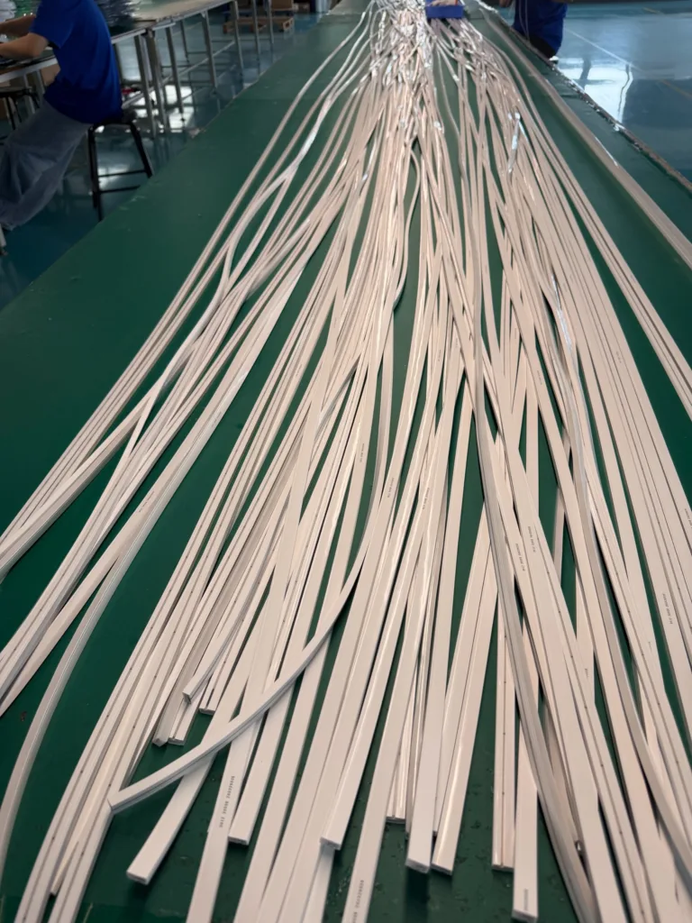
How Does Silicone Extrusion Impact Final Product Quality?
For LED Silicone Neon Flex, the silicone housing isn't just a protective shell—it's a precision optical component that must maintain clarity, color accuracy, and mechanical integrity for 5+ years. Poor extrusion control introduces defects that won't show up in factory testing but will destroy your project in the field.
Silicone extrusion involves feeding platinum-cure liquid silicone rubber (LSR) through a heated die to form continuous profiles, followed by UV or thermal curing. The failure-critical factors are: molecular chain integrity (excessive shear heat causes chain scission), cross-link density uniformity (affects compression set and yellowing resistance), and contamination control (VOCs and unreacted monomers migrate to LED surfaces, causing phosphor poisoning).

Extrusion Temperature and Shear Stress
Premium silicone compounds are engineered for extrusion at 160~180°C. But here's the problem: if the extruder barrel isn't temperature-zoned correctly, localized hot spots can reach 200°C+. At this temperature, polysiloxane chains break. Molecular weight drops. Mechanical properties degrade.
The immediate symptom is reduced tear strength (drops from 28 kN/m to 18 kN/m). The long-term consequence is accelerated yellowing and surface degradation. I've tested competitor products where UV aging caused 500% faster color shift compared to properly extruded silicone—purely due to molecular damage during manufacturing.
Cross-Link Density: The Cure You Can't See
Platinum-cure silicone curing involves complex chemistry. Vinyl groups on the polymer react with Si-H cross-linkers, catalyzed by platinum complexes. Complete curing requires:
- Proper catalyst concentration (typically 10~50 ppm Pt)
- Uniform temperature distribution (±5°C across die exit)
- Sufficient residence time in the curing oven/UV chamber
Under-cured silicone feels normal initially. But under compression (like in mounting clips), it exhibits high compression set—permanent deformation. After thermal aging, uncured oligomers migrate to the surface, causing tackiness and attracting dust.
Over-cured silicone becomes brittle. Impact resistance drops. In cold environments (-40°C), it can crack.
Optical Refractive Index Control
For uniform light emission, silicone refractive index must match the LED encapsulant (RI ~1.41). If the housing RI drifts to 1.38 or 1.45, internal reflection changes. You get hot spots—bright zones directly over LEDs