

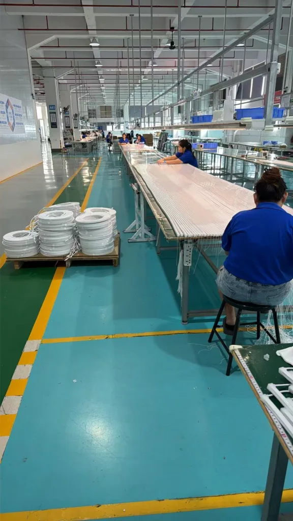
When most people ask "How are LED strips manufactured?", they're curious about the production flow. But here's what experienced contractors actually worry about: whether your LED strips will fail in batches six months after installation—and the answer isn't found at the job site. It's hidden in the production line, in process details you'll never see listed in any spec sheet.
The real question isn't how LED strips are made—it's whether the manufacturer controls every microscopic variable that determines if your building façade will still look uniform two years from now. Because LED strips aren't products. They're systems. And when one invisible step goes wrong during manufacturing, it becomes your expensive field replacement problem later.
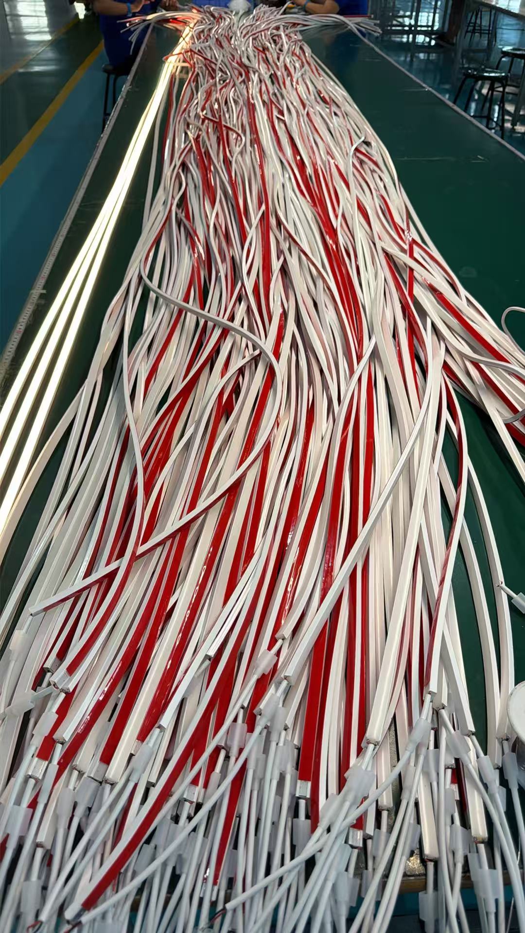
I've watched projects fail not because the strips stopped working, but because different production batches—all passing the same quality tests—looked visibly different when installed side by side. Let me walk you through what actually happens during LED strip manufacturing, and more importantly, where things go wrong when nobody's watching closely enough.
What are the core stages of LED strip manufacturing?
At Shenzhen Alister, we break LED strip manufacturing into five critical phases: component preparation, PCB assembly, LED integration, encapsulation, and final testing. But the real story isn't in these steps themselves—it's in how tightly we control variations between them.
The manufacturing process isn't just about assembling parts. It's about maintaining consistency across thousands of meters, multiple batches, and months of production time. That's where most factories fail, and where I've seen the most expensive project disasters happen.
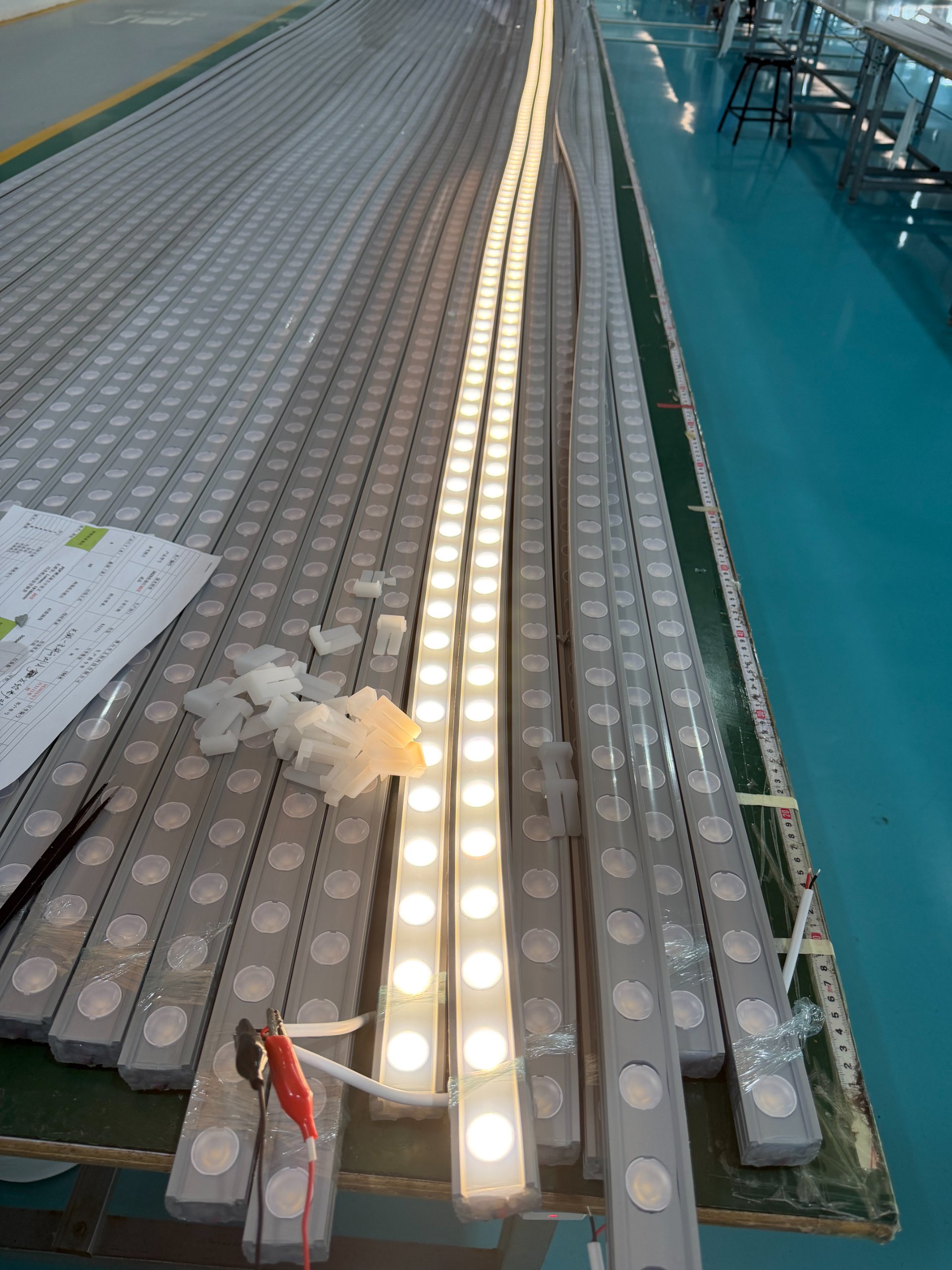
The five manufacturing phases that determine long-term reliability
| Phase | What Happens | Hidden Risk Most People Miss |
|---|---|---|
| 1. Component Sourcing | LED chips, PCB boards, copper traces, resistors, and protective materials are selected and batch-tested | LED bins change between orders. Same color temperature on paper ≠ same visual appearance |
| 2. PCB Preparation | Copper-clad FR4 boards are cut, etched, and coated with solder mask. Trace width and copper thickness determine current capacity | Insufficient copper thickness = heat accumulation = premature LED degradation |
| 3. SMT Assembly | Surface-mount technology machines place LEDs, resistors, and ICs onto PCB with 0.05mm precision | If reflow soldering temperature curve isn't locked, solder joints develop micro-cracks over time |
| 4. Encapsulation | Silicone extrusion or PU potting seals the strip for IP65/IP67/IP68 protection | Material incompatibility between silicone and adhesive causes yellowing after 12-18 months |
| 5. Testing & QC | Electrical testing (voltage drop, color temperature, lumen output) and aging tests | Lab tests run for 8 hours. Commercial projects run 16+ hours daily. Temperature buildup is never simulated |
Here's the part that matters for large-scale projects: the manufacturing process you see in factory tours is usually the "ideal state" version. The version where all variables are controlled. But I've audited dozens of factories, and the gap between their best-case process and their average weekday process is often the difference between a five-year lifespan and a two-year failure rate.
Why does LED bin selection during manufacturing affect your project years later?
Most people think LEDs either work or they don't. But here's the truth: LEDs are sorted into "bins" after production based on tiny differences in brightness, color temperature, and forward voltage. A single LED production run can generate 20+ different bins. And when your strip manufacturer switches bins mid-project, you get color shifting.
I saw this destroy a $400,000 commercial façade project. First batch: perfect. Second batch: same specs on paper. But when installed, the building showed visible yellow and white bands at night. The fix cost more than the original strips.

How LED binning impacts long-term consistency
During manufacturing, LED suppliers test each chip and assign it to a bin based on:
- CCT (Correlated Color Temperature): The "warmth" or "coolness" of white light
- Luminous Flux: Total light output in lumens
- Forward Voltage (Vf): Electrical characteristics that affect power consumption
- CRI (Color Rendering Index): How accurately colors appear under the light
The problem? Even within the "3000K warm white" category, there are sub-bins with measurable differences. A 3-step MacAdam ellipse difference is invisible in isolation but becomes obvious when two batches are installed adjacent to each other.
Critical Manufacturing Control Point: Reputable manufacturers lock a specific bin for your entire project and maintain buffer stock. At Alister, we purchase 15-20% excess inventory per project and store it under controlled conditions to guarantee batch consistency for follow-up orders.
But most budget factories? They use whatever bin is cheapest that week. Your 5000-meter project gets split across three different bins, and you discover the problem only after installation.
How does reflow soldering temperature determine whether your strips fail after 10,000 hours?
This is where things get technical, but stay with me—because this is where most "mysterious failures" actually originate. Reflow soldering is the process where surface-mount LEDs are bonded to the PCB using solder paste and high heat. The temperature profile must follow a precise curve: preheat, soak, reflow, and cooling.
When this curve varies by even 10-15°C between production runs, you create invisible stress fractures in solder joints. These joints pass initial testing. They survive shipping. They work perfectly for months. Then thermal cycling causes them to crack, and entire sections go dark.
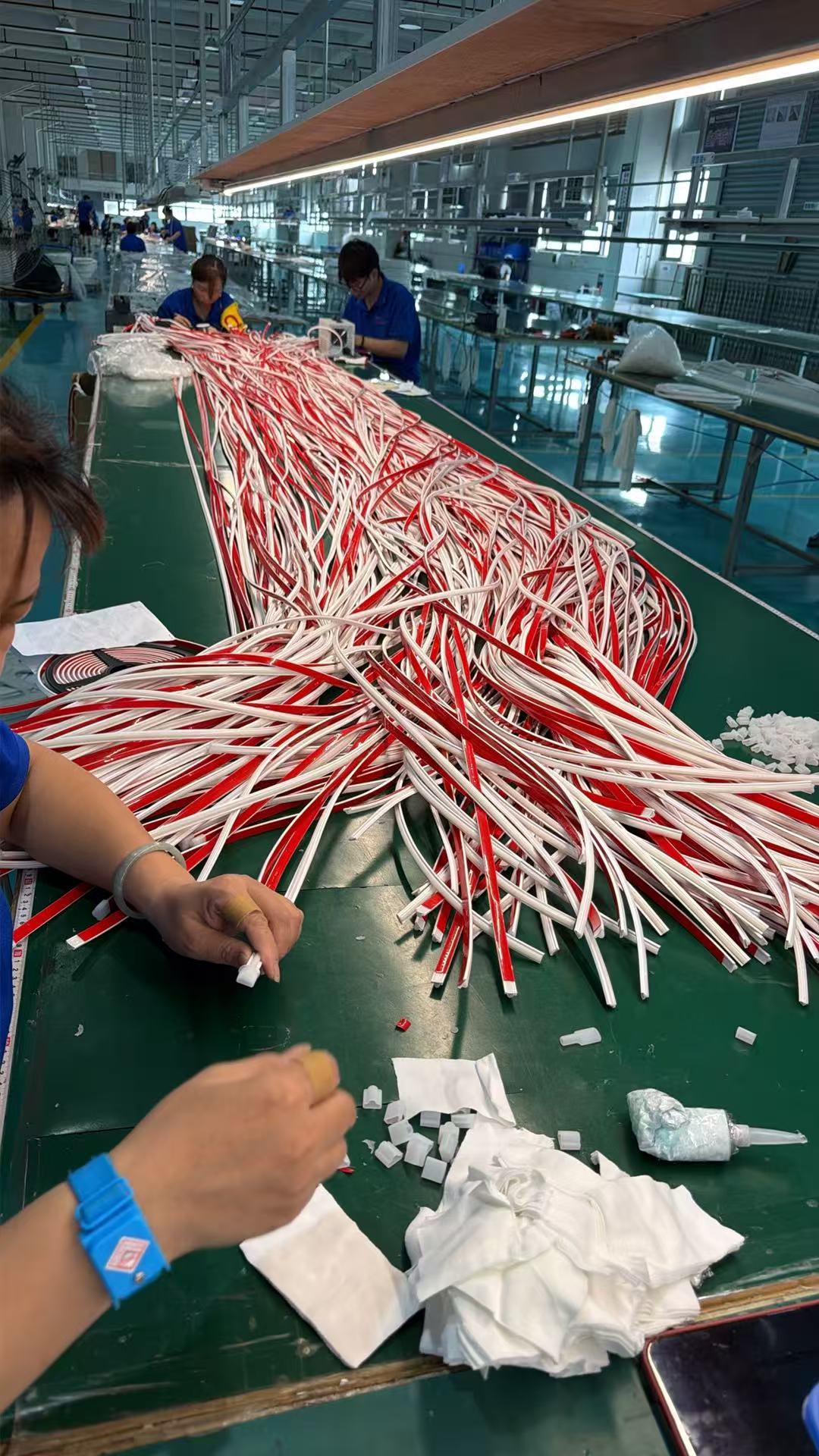
The three-stage thermal profile that prevents latent failures
| Stage | Temperature Range | What Goes Wrong If Deviated |
|---|---|---|
| Preheat (150-180°C) | Gradually raises PCB and component temperature | Too fast = thermal shock damages LED internal structure |
| Soak (180-200°C) | Activates flux in solder paste and removes oxidation | Insufficient soak = poor wetting = weak mechanical bond |
| Reflow Peak (240-260°C) | Melts solder and forms metallurgical bond | Overheating degrades LED phosphor coating and gold wire bonds |
| Cooling (<6°C/sec) | Controlled cooldown prevents thermal stress | Rapid cooling causes internal strain and microfractures |
Here's what I learned after investigating hundreds of field failures: the factories that fail most often are the ones that run their reflow ovens slightly too hot to increase production speed. They save 15 seconds per board. You lose 2 years of product life.
At Shenzhen Alister, every production run includes a thermal profiling test where we attach thermocouples to actual PCBs and record the entire temperature curve. If any deviation exceeds ±5°C from our locked profile, we recalibrate before continuing. This costs us time. But it's why our warranty claims are below 0.3%.
Why does PCB copper thickness matter more than most specs sheets suggest?
When you look at an LED strip datasheet, you'll see voltage, wattage, and IP rating. What you won't see is the copper weight (measured in ounces per square foot) or trace width. And that's a problem, because these invisible design choices control how much heat your strips generate during operation.
I once reverse-engineered a competitor's strip that claimed identical specs to ours. Their copper was 1oz. Ours was 2oz. Under identical load conditions, their strip ran 18°C hotter. That temperature difference alone cuts LED lifespan by approximately 40%.

How copper weight and trace design control operational temperature
LED strips generate heat from three sources:
- LED junction heat (from electrical-to-photon conversion inefficiency)
- Resistor dissipation (voltage regulation generates waste heat)
- Trace resistance (thin copper = higher resistance = I²R heating)
When manufacturers cut costs, they reduce copper thickness. A 1oz copper PCB has half the conductivity of a 2oz board. Under continuous 16-hour commercial operation, that difference compounds:
- 1oz copper @ 24V, 14.4W/m: surface temperature reaches 65-70°C
- 2oz copper @ 24V, 14.4W/m: surface temperature stays below 50°C
Why does this matter? Because every 10°C increase in junction temperature reduces LED lifespan by approximately 50%. It's not the heat that kills your project—it's the cumulative thermal stress over 20,000+ operating hours.
Critical Manufacturing Control Point: Professional-grade LED strips use 2oz or even 3oz copper, wider traces (minimum 2mm for high-power runs), and strategic thermal vias to dissipate heat into the substrate. Cheap strips use 0.5oz or 1oz copper because it's easier to etch and costs less.
At Shenzhen Alister, we use 2oz copper as our baseline for all commercial-grade silicone neon flex strips. For outdoor façade projects exceeding 10m continuous runs, we upgrade to 3oz copper and implement parallel trace routing to further reduce voltage drop and heat concentration.
What encapsulation materials actually prevent water ingress for 5+ years?
IP67 or IP68 ratings mean the strip passed a short-term immersion test. But here's what those ratings don't tell you: whether the encapsulation material will remain compatible with the PCB, adhesive, wire insulation, and LED phosphor coating over thousands of thermal cycles. Most waterproofing failures aren't instant leaks—they're material degradation.
I've seen strips pass 1000-hour salt spray tests, then develop yellowing and surface tackiness after 18 months of outdoor exposure. The silicone wasn't the problem. The adhesive underneath was releasing VOCs that migrated through the silicone and degraded it from within.
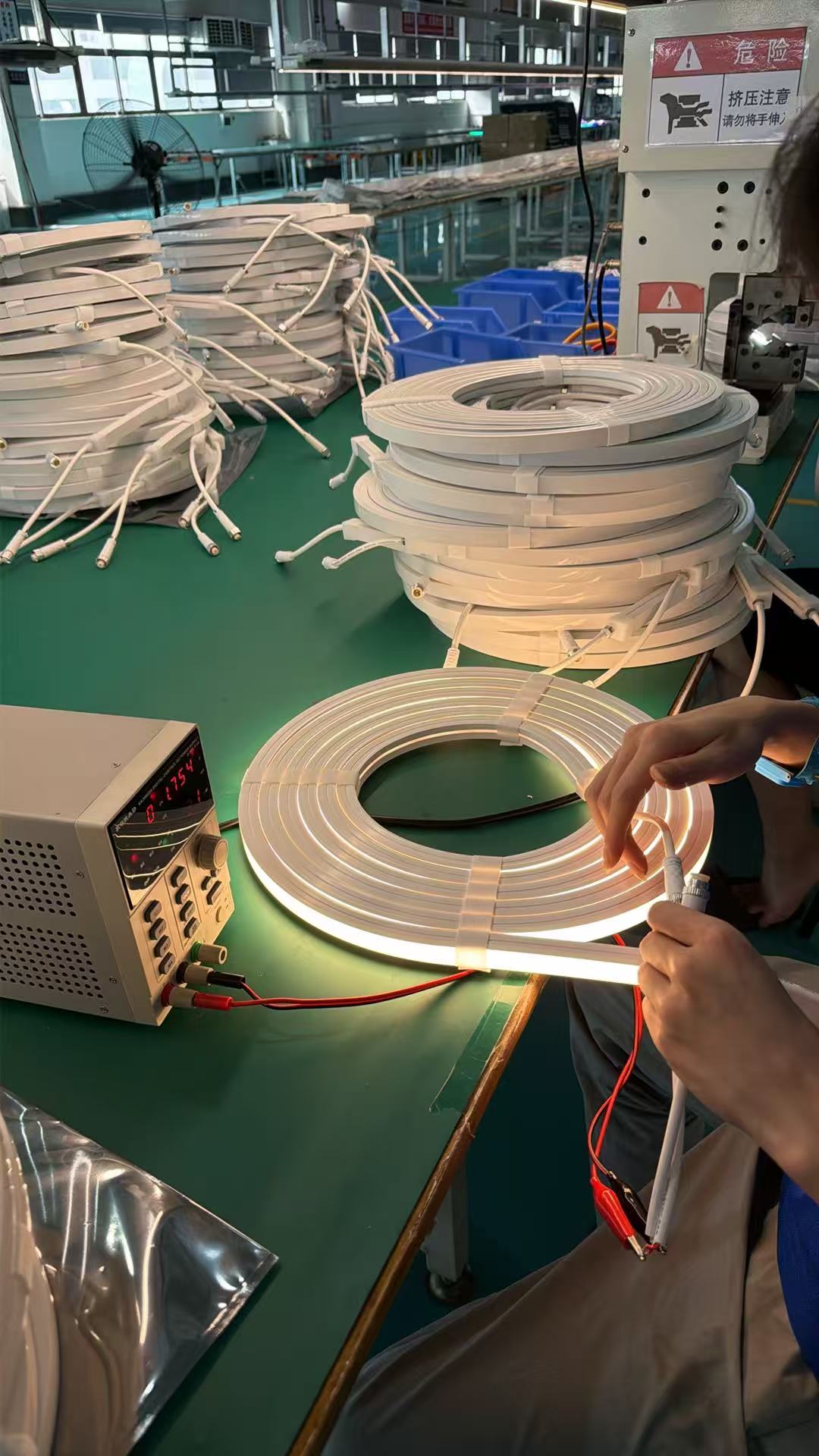
The three-layer system that determines waterproof longevity
| Layer | Material | Failure Mode if Incompatible |
|---|---|---|
| Base Adhesive | Acrylic or silicone PSA (pressure-sensitive adhesive) | Releases plasticizers or volatile organics that attack silicone layer above |
| Primary Encapsulation | PU potting, epoxy resin, or silicone extrusion | PU yellows under UV. Epoxy becomes brittle in freeze-thaw cycles. Low-grade silicone cracks at cold temperatures |
| Outer Protective Layer | UV-stabilized silicone or TPU (thermoplastic polyurethane) | Incompatible silicone grades cause delamination at material boundaries |
The most dangerous failure mode is material migration: small molecules from one layer diffuse into another over time, changing physical properties. This doesn't show up in 48-hour water immersion tests. It shows up 12-24 months later as:
- Yellowing or discoloration
- Surface stickiness (adhesive breaking down)
- Cracking at junction points
- Water vapor permeability increasing over time
Critical Manufacturing Control Point: At Shenzhen Alister, we use 100% food-grade platinum-cured silicone (LSR - Liquid Silicone Rubber) for our neon flex products. Unlike peroxide-cured silicone, platinum-cured silicone produces no acidic byproducts during curing, eliminating the risk of long-term chemical attack on LED phosphor coatings or copper traces.
We also run accelerated aging tests at 85°C/85% RH for 2000+ hours, then perform adhesion pull tests and visual inspection. Any formulation showing >5% adhesion loss is rejected, regardless of whether it meets basic IP ratings.
How does mechanical stress during manufacturing create delayed failures?
This is the most overlooked aspect of LED strip manufacturing: mechanical stress isn't just created during installation or shipping. It's introduced during production itself. And when stress accumulates at material boundaries, it creates microfractures that propagate slowly over time until catastrophic failure occurs.
I investigated a project where strips started failing randomly after 8-12 months. No pattern. No environmental correlation. When we cross-sectioned failed units, we found hairline cracks in the LED solder joints—but only on strips manufactured during a specific two-week period. It turned out the silicone extrusion line had been running slightly too fast, creating excessive pull force on the PCB during the curing process.
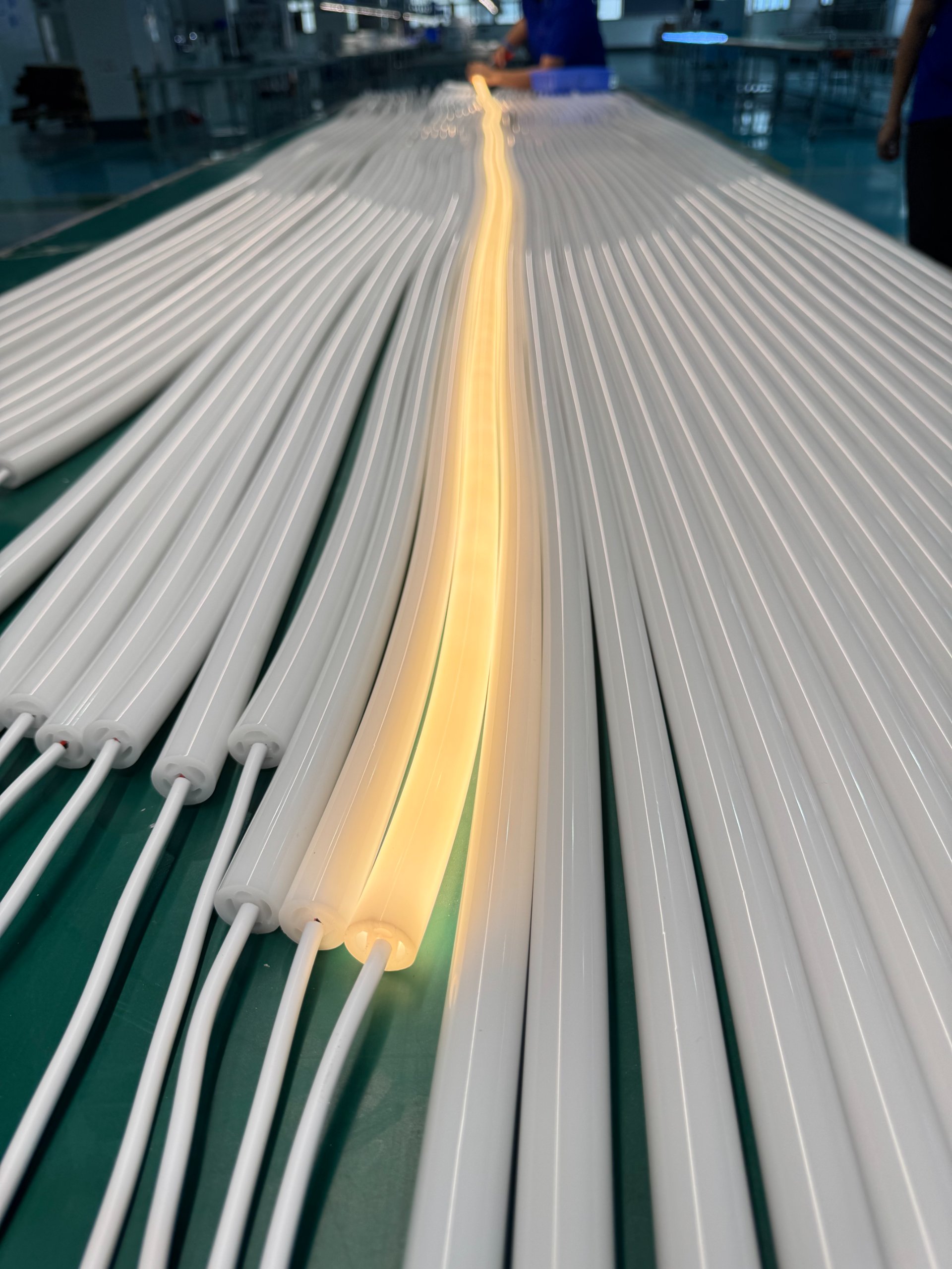
The four manufacturing steps that introduce hidden mechanical stress
-
SMT Pick-and-Place Pressure: Component placement machines apply 2-4N of force when pressing LEDs onto PCB. Excessive force can compress the LED package, creating internal stress on gold wire bonds.
-
Reflow Thermal Expansion: Different materials expand at different rates. When PCB (CTE ~17 ppm/°C), copper (CTE ~16.5 ppm/°C), LED ceramic substrate (CTE ~6-7 ppm/°C), and solder (CTE ~25 ppm/°C) all heat and cool together, they create shear stress at interfaces.
-
Encapsulation Curing Shrinkage: Silicone shrinks 0.5-2% as it cures. PU potting compounds shrink 2-4%. This creates tensile stress on solder joints and PCB traces. If the silicone layer is too thick or cures too quickly, localized stress can exceed the fatigue limit of solder joints.
-
Reel Winding Tension: When finished strips are wound onto reels, improper tension creates bending stress on the PCB. Copper traces near the neutral axis handle this well, but traces near the outer edge experience cyclical strain.
Critical Manufacturing Control Point: Professional manufacturers control mechanical stress through:
- Calibrated nozzle pressure on pick-and-place machines
- Slow, controlled reflow cooling rates
- Thin-layer silicone application (multiple passes if needed)
- Precision tension control during reel winding (<500g for standard strips)
At Shenzhen Alister, we implement strain relief design in our PCB layouts, placing solder pads slightly oversized and using copper tear-drop shapes at trace-to-pad transitions. This distributes mechanical stress over a larger area and reduces crack propagation risk by approximately 60% compared to standard right-angle PCB designs.
Conclusion
LED strip manufacturing isn't about making lights turn on—it's about controlling hundreds of invisible variables so they're still turning on five years from now, looking exactly like they did on day one. The factories that survive in this industry are the ones that treat manufacturing as a continuous battle against entropy, material drift, and process variation. Because in the end, the most expensive manufacturing defects are the ones you discover two years after installation.