


Lighting projects fail at final acceptance far more often than they fail at the factory. If you are specifying, procuring, or commissioning LED lighting at scale, the question of how an LED is manufactured is not an academic exercise — it is a project-risk question. Understanding each manufacturing stage tells you exactly where the variables live, and which variables can quietly destroy your lighting project's visual outcome.
An LED is manufactured through a sequential chain of tightly controlled processes: semiconductor wafer preparation, epitaxial growth, wafer processing, die testing, dicing, packaging, and binning. Each stage introduces variables that affect the final device's optical and electrical behavior. For project buyers and procurement teams, understanding this chain is not a technical curiosity — it is the foundation of component-control strategy, supplier qualification, and specification writing.
Most procurement teams treat LED manufacturing as a black box. They compare nominal specifications, approve a sample, and assume the mass-production result will match. That assumption is where large projects go wrong. The sections below trace every critical manufacturing stage and explain what it means for your next project.
What Happens During Semiconductor Wafer Preparation?
Most buyers never see a wafer. But the semiconductor wafer is the foundation of every LED that enters your project, and its preparation directly determines the range of variation that follows downstream.
Semiconductor wafer preparation establishes the substrate and base material structure on which LED-active semiconductor layers will be grown. For common visible LEDs — particularly blue and white GaN-based devices — the wafer quality, crystal structure, and surface preparation define the operating envelope of every die that will eventually be cut from it.

Why Wafer Quality Matters for Project Buyers
Project buyers have almost no direct visibility into this stage. That is the point. Because you cannot see it, you must control it indirectly.
Here is what wafer preparation affects downstream:
- Wavelength uniformity — Small variations in semiconductor layer composition shift the emitted wavelength distribution, which affects perceived color temperature in the finished LED strip.
- Electrical characteristics — Forward voltage behavior traces partly back to material quality at this stage.
- Yield distribution — Wafer quality affects how many dies fall into premium versus lower performance bins during later sorting.
- Batch-to-batch consistency — Two production lots can use LEDs that both pass specification but come from wafers with different material batches, producing subtly different visual results.
The project-level risk is structural. A procurement specification that defines only package size and nominal color temperature does not reach back to wafer-level variables at all. The specification may look precise while leaving the most fundamental manufacturing variables completely uncontrolled.
What the Project Should Control Instead
You cannot realistically audit a semiconductor wafer supplier from the lighting project side. What you can do:
- Require LED source traceability — The LED strip manufacturer should be able to identify which LED package manufacturer and which production lot supplied their devices.
- Lock the approved component source — Once a sample is approved, specify that the LED package manufacturer and component source cannot change without documented approval.
- Treat "equivalent chip" claims with formal scrutiny — A claim that "we use the same chip" is only meaningful if it refers to the same approved package and production configuration, not merely the same nominal semiconductor material.
The wafer stage is where project risk originates. It is controlled — or it is not — long before a single LED strip reaches your site.
What Is Epitaxial Growth and Why Does It Create Batch Variation?
Epitaxial growth is one of the most process-sensitive stages in LED manufacturing. It is also the stage most likely to produce batch-to-batch variation that falls within specification while still producing a visually inconsistent result at scale.
During epitaxial growth, semiconductor layers are deposited onto the prepared wafer under precisely controlled temperature, pressure, and gas-flow conditions. For GaN-based LEDs, this process creates the quantum-well structures that define the device's light-emitting behavior.
The Critical Distinction: Within-Specification Variation
This is the concept that causes the most damage on large projects, and it deserves direct explanation.
An LED can pass its manufacturer's quality test while still behaving differently from another LED produced in a separate epitaxial run.
Both LEDs are technically acceptable. Both meet the stated specification. But the distribution of their optical output — particularly wavelength and color temperature — can sit at different positions within the allowed tolerance range.
When thousands of these LEDs are assembled into linear strips and installed continuously across a façade, ceiling, or architectural detail, the difference between two within-spec production lots can become visible.
Consider what epitaxial variation can affect:
| Parameter | Effect of Epitaxial Variation | Project Consequence |
|---|---|---|
| Peak wavelength | Shifts perceived color of blue pump LED | Color temperature variation in white LED strips |
| Quantum well structure | Affects optical efficiency | Brightness variation between batches |
| Layer thickness uniformity | Alters forward voltage distribution | Electrical performance difference |
| Wafer-to-wafer consistency | Different binning outcomes per production run | Visual inconsistency at installation |
The Specification Gap This Creates
A specification that states "3000 K ± 150 K" may technically accommodate two production lots that look visually different under installation conditions.
The tolerance is not wrong. It is simply not sufficient on its own to guarantee visual uniformity for a continuous architectural installation.
What the specification needs in addition:
- A MacAdam ellipse or equivalent color consistency requirement, defined for the specific application.
- A binning requirement that narrows the acceptable range to what the eye can actually tolerate under real installation conditions.
- A production-lot consistency requirement ensuring that strips installed adjacently come from controlled production batches.
Epitaxial growth cannot be reversed or corrected after the wafer is processed. The variation it introduces propagates through every subsequent stage. Controlling it requires defining the output requirements before procurement, not after installation.
How Does Wafer Processing Turn Semiconductor Layers Into LED Dies?
After epitaxial growth, the wafer undergoes a series of semiconductor fabrication operations that create the functional LED device structure. This stage transforms a layered semiconductor material into addressable electrical and optical components.
Typical wafer processing operations include lithography, etching, deposition, metallization, electrical contact formation, passivation, and wafer-level electrical testing. Each step is tightly sequenced and controlled.
At this point, the risk profile begins to shift. The earlier stages introduced material variation. Wafer processing introduces device variation — differences in how individual LED dies perform electrically and optically, even on the same wafer.
From Material to Device: Where the Distribution Widens
No wafer produces perfectly identical dies. Process uniformity across a wafer has physical limits. Dies near the wafer edge typically show different characteristics from dies near the center. Processing equipment introduces its own micro-variation.
The result is a distribution of device performance, not a single uniform output.
This is not a manufacturing failure. It is a physical reality. The manufacturing process is designed to keep that distribution within a controlled range, and subsequent testing and binning are designed to characterize and sort that distribution into useful product groups.
For a project buyer, the implication is:
The device coming out of wafer processing is already a distribution, not a fixed point. The question is how that distribution is subsequently classified and controlled.
What This Means for Strip-Level Assembly
An LED strip manufacturer assembles thousands of individual dies (in packaged form) into finished products. If the dies entering their assembly process come from multiple bins, or from uncontrolled production lots, the strip output will reflect that underlying variation.
A rigorous strip manufacturer manages this by:
- Sourcing LEDs from controlled lot production.
- Using matched bins within a production run.
- Segregating production batches for traceability.
A less rigorous manufacturer may mix available stock.
The finished strip may still pass a nominal specification test. But its visual consistency — particularly across large, continuous installations — will be lower.
This is why, when I evaluate a strip supplier for a significant project, I do not only ask what their production tests cover. I ask how they manage the incoming LED lot and what controls prevent bin mixing across a single project's production run.
What Is LED Binning and Why Does It Matter More Than the Specification?
LED binning is one of the most underappreciated and most consequential aspects of LED manufacturing for project buyers. Understanding it properly changes how you write specifications, evaluate samples, and qualify suppliers.
After wafer processing and separation, LED packages are tested and sorted — "binned" — according to measured performance characteristics including forward voltage, optical output, and wavelength or color temperature.
Binning is a classification system, not a pass/fail judgment. Two LEDs can both pass commercial quality requirements while belonging to different bins and therefore producing different optical outputs.
The Binning Risk in Large Projects
I have seen this pattern cause real project disputes. Here is how it unfolds at scale.
A project specifies 3000 K LED strip. The supplier provides a sample. The sample looks correct against a reference under controlled conditions. Mass production begins. The supplier sources LEDs from available stock — all within the stated 3000 K tolerance. But the stock includes devices from different bins within that tolerance range.
After installation:
- Sections installed at different dates show subtle but noticeable differences.
- Under certain ambient conditions — evening, overcast sky, directional observation angles — the variation becomes visible.
- No individual LED is defective. No individual strip fails a test.
The project still has a problem.
What a Proper Binning Requirement Looks Like
For architectural and commercial projects where visual continuity matters:
| Requirement Type | What to Specify | Why It Matters |
|---|---|---|
| Color consistency | MacAdam 3-step ellipse or tighter | Limits visible color variation between adjacent LEDs |
| Color temperature range | Narrower than standard tolerance (e.g., ±100K vs ±150K) | Reduces bin spread within a project's production |
| Bin mixing control | Single-bin or adjacent-bin only within one project run | Prevents visible step changes between installation sections |
| Lot consistency | All strips in one installation zone from same production lot | Ensures physical traceability and visual uniformity |
A specification that simply reads "3000 K, CRI 80+" defines a product category. It does not define a binning configuration. For a small, non-critical installation, that may be acceptable. For 18 km of continuous architectural Silicone LED Neon Flex on a landmark façade, it is not.
How Does LED Packaging Transform a Die Into a Usable Light Source?
After the wafer is diced into individual semiconductor dies, the bare die must be packaged before it can be used in any practical lighting application. LED packaging is a manufacturing stage in its own right, and it introduces another layer of variables that affect the finished product's performance.
Depending on the LED design, packaging operations can include die attachment to a substrate or lead-frame, electrical wire bonding or flip-chip connection, encapsulation, phosphor application or mixing, optical lens formation, and final package-level testing.
For white LEDs — which is the vast majority of what enters commercial LED strip products — the phosphor system applied during packaging is particularly critical. The phosphor converts the blue pump light from the semiconductor die into the broader spectrum that produces white light. The phosphor formulation, application uniformity, and curing process directly affect:
- Color temperature output
- Color rendering index
- Color consistency across packages
- Long-term color stability under thermal stress

The "Same Chip" Problem
This is where one of the most common procurement misunderstandings occurs.
A supplier states: "We use the same chip as Brand X."
This statement may be technically accurate and commercially misleading at the same time.
The die may come from the same semiconductor manufacturer. But the package manufacturer — the company that attaches, connects, encapsulates, and phosphor-coats the die — may be completely different.
The package manufacturer's process determines:
- Phosphor consistency
- Encapsulant quality and UV stability
- Thermal resistance of the assembly
- Mechanical reliability under cycling
- Color maintenance over lifetime
Two finished LED packages using "the same chip" from different package manufacturers can produce different optical results and different lifetime behavior.
For project specification purposes, the correct requirement is not just the semiconductor source. It is the approved LED package — identified by manufacturer, part number, and production configuration — that was used for the approved sample.
What Is the Risk of Uncontrolled LED Source Substitution?
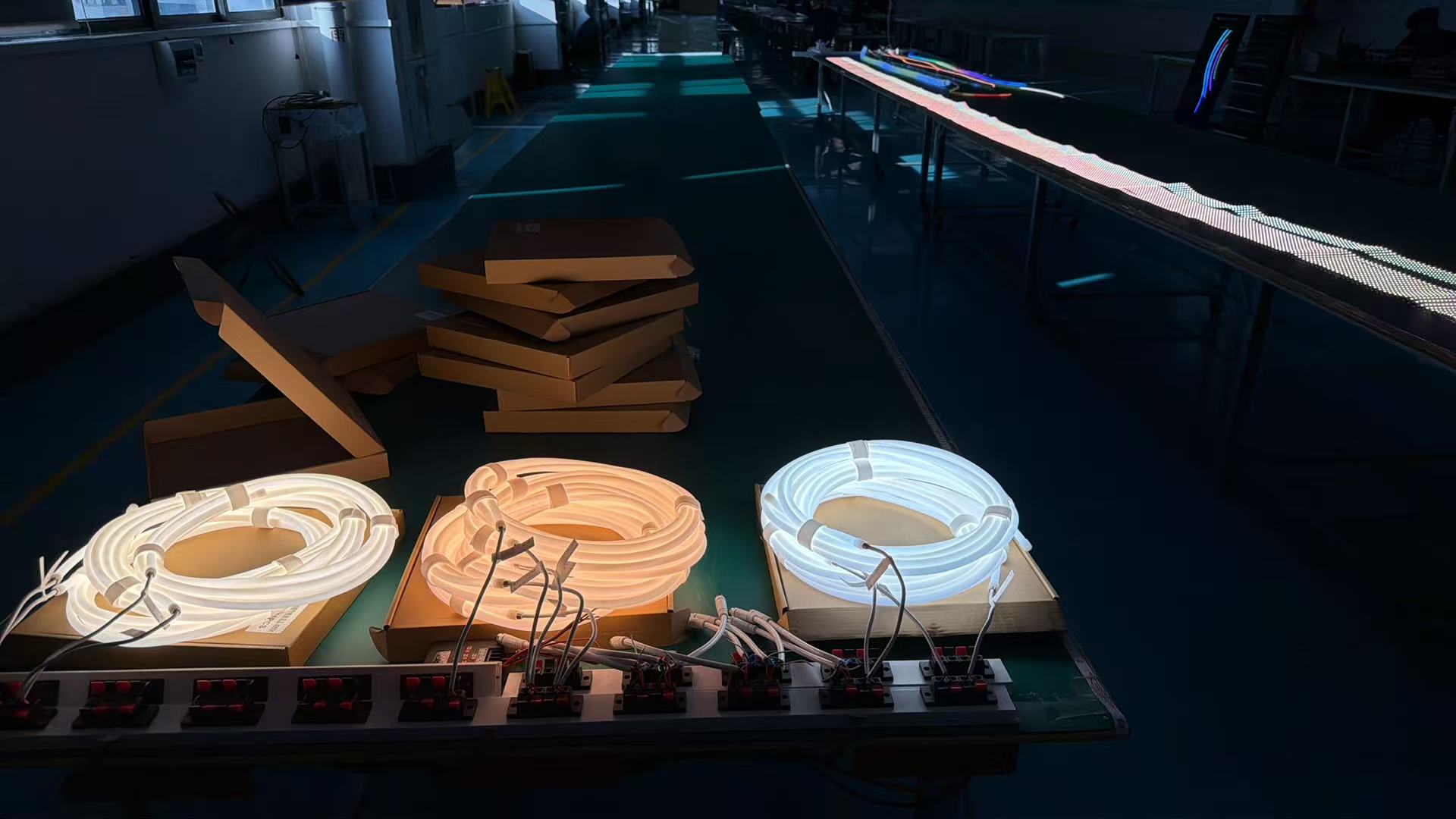
Uncontrolled LED source substitution is, in my experience, the single most common cause of visual quality disputes on large LED lighting projects. It combines multiple manufacturing variables — packaging, binning, phosphor — into a single undocumented change that often occurs after sample approval and before delivery.
The substitution typically happens for commercially rational reasons. An LED package becomes temporarily unavailable. A cost opportunity arises. A "technically equivalent" alternative is identified internally by the supplier. The new component passes the supplier's own internal test. No formal notification is issued. Production continues.
How the Risk Escalates Through Project Phases
The cost of discovering an uncontrolled substitution scales sharply with when it is discovered:
| Discovery Point | Typical Corrective Action | Cost Level |
|---|---|---|
| During sample approval | Reject substitute, request correct sample | Low |
| Before mass production starts | Halt production, re-qualify component | Moderate |
| During production, before delivery | Segregate affected lots, replace if necessary | Moderate–High |
| After delivery, before installation | Sort and replace affected product | High |
| After installation, before commissioning | Potential removal and reinstallation | Very High |
| After commissioning, at final acceptance | Contractual dispute, potential full replacement | Extremely High |
This escalation is the characteristic pattern of uncontrolled manufacturing risk. The problem does not get more expensive because the LED itself changed dramatically. It gets more expensive because the cost of correction increases at each project phase, while the technical problem itself remains essentially the same.
The Contractual Trap
The most damaging scenario is the one where both parties are correct.
- The supplier: "The replacement LED meets the specification."
- The contractor: "The installed lighting does not match the approved sample."
- The procurement team: "The package designation and color temperature are the same."
- The designer: "The visual result is not acceptable."
None of these statements is false.
The failure occurred earlier: the project never defined what constituted an approved manufacturing configuration. The specification defined a performance category. It did not lock the manufacturing variables that determine whether that performance category produces a consistent visual result.
The resolution requires:
- Change-control clauses — explicitly requiring supplier notification and approval before any LED source, package, or phosphor-system change.
- Sample-to-production equivalence requirements — stating that mass production must use the same LED configuration as the approved sample, not merely a nominally equivalent alternative.
- Traceability requirements — requiring production lots to be identified so that any affected batches can be isolated and evaluated.
Frequently Asked Questions
What does LED binning mean in practice for a lighting project?
Binning sorts LED packages by measured performance — particularly color temperature, forward voltage, and optical output. Two LEDs from different bins can both pass a nominal specification while producing visually different results at scale. For large or continuous architectural installations, defining the required bin range is as important as defining the nominal color temperature.
Can two LED strips have the same specification but look different?
Yes. If the strips use LEDs from different production lots, different bins, or different package manufacturers — even with identical nominal specifications — they can produce subtly different visual results. This is most noticeable in continuous installations observed under consistent ambient conditions. Visual consistency requires bin-level control, not only nominal specification control.
What certifications should I verify when purchasing LED strips for a commercial project?
Relevant certifications depend on the destination market and application. CE and RoHS are typically required for European markets. UL is relevant for the North American market. SAA applies to Australia and New Zealand. SASO is required for Saudi Arabia. Buyers should request and independently verify current certification documentation. Certifications are documents that require active verification — not assumptions.
What is the difference between a LED die, a LED package, and a LED strip?
A die is the bare semiconductor component cut from the wafer. A package is the die after it has been assembled with electrical connections, encapsulant, and phosphor into a usable component. A LED strip is the finished product in which packaged